← → to move between modules
03 / 09 · Input
Six buttons over I²C
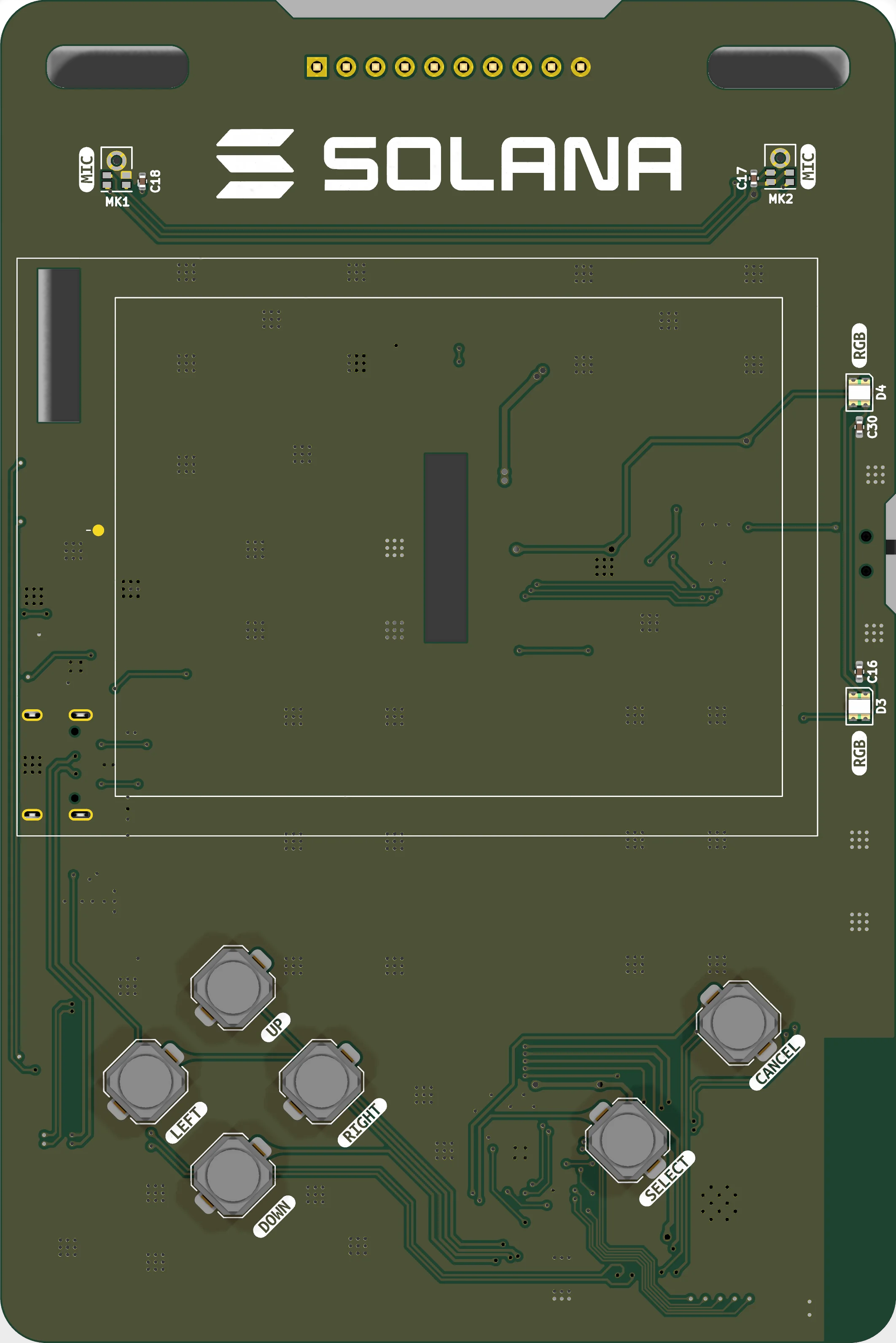
A D-pad plus select and cancel, read through a TCA9534 expander rather than GPIO.
- Buttons
- 6 tactile
- Expander
- TCA9534 (U10)
- Address
- 0x20
- Interrupt
- GPIO4, active LOW
The six buttons are the only user controls on the badge, and none of them touch an ESP32 pin. They land on P0–P5 of U10, a TCA9534 8-bit I/O expander sitting on the shared I²C bus at address 0x20. That buys back six GPIO at the cost of a bus transaction per read.
Silkscreen on the front face labels them as a directional cluster — UP, LEFT, RIGHT, DOWN on the left, SELECT and CANCEL on the right — but the expander has no idea about that. Firmware reads the input port register and gets bits 0–5, active LOW.
You do not have to poll. U10 asserts its open-drain INT on GPIO4 whenever an input changes, so the usual pattern is to sleep on the interrupt and only touch the bus when something moved. P6 and P7 are unconnected.
Pins
| Pin | Net | Role | Function |
|---|---|---|---|
| GPIO4 | PBINT | INT | Change interrupt from U10 pin 13. Active LOW, open-drain. |
| GPIO9 | SCL | I²C CLK | Shared clock. 2K2 pull-up R10 to 3V3. |
| GPIO10 | SDA | I²C DATA | Shared data. 2K2 pull-up R8 to 3V3. |
Parts
- PB1 SW_Push — UP P0 · bit 0
- PB2 SW_Push — LEFT P1 · bit 1
- PB3 SW_Push — RIGHT P2 · bit 2
- PB4 SW_Push — DOWN P3 · bit 3
- PB5 SW_Push — SELECT P4 · bit 4
- PB6 SW_Push — CANCEL P5 · bit 5
- U10 TCA9534 I/O expander — back face, address 0x20 (A2/A1/A0 all to GND)
Firmware
constexpr int     PIN_BUTTON_INT    = 4;
constexpr uint8_t TCA9534_ADDR      = 0x20;
constexpr bool    BUTTON_ACTIVE_LOW = true;

// Expander bit per key — measured, not assumed.
constexpr uint8_t BTN_UP    = 0;  // P0, PB1
constexpr uint8_t BTN_LEFT  = 1;  // P1, PB2
constexpr uint8_t BTN_RIGHT = 2;  // P2, PB3
constexpr uint8_t BTN_DOWN  = 3;  // P3, PB4
constexpr uint8_t BTN_A     = 4;  // P4, PB5 — SELECT
constexpr uint8_t BTN_B     = 5;  // P5, PB6 — CANCEL
Notes
- Note the bit order: DOWN is at P3, after LEFT and RIGHT — not the up/down/left/right that reads naturally. Firmware that assumes otherwise still works, it just delivers the wrong action.
- Solana OS exposes these to Lua as "up", "left", "right", "down", "a" and "b"; the test kit refers to them by port bit.
- Flip to the back face to see U10 and its pull-up array next to the ESP32 module.