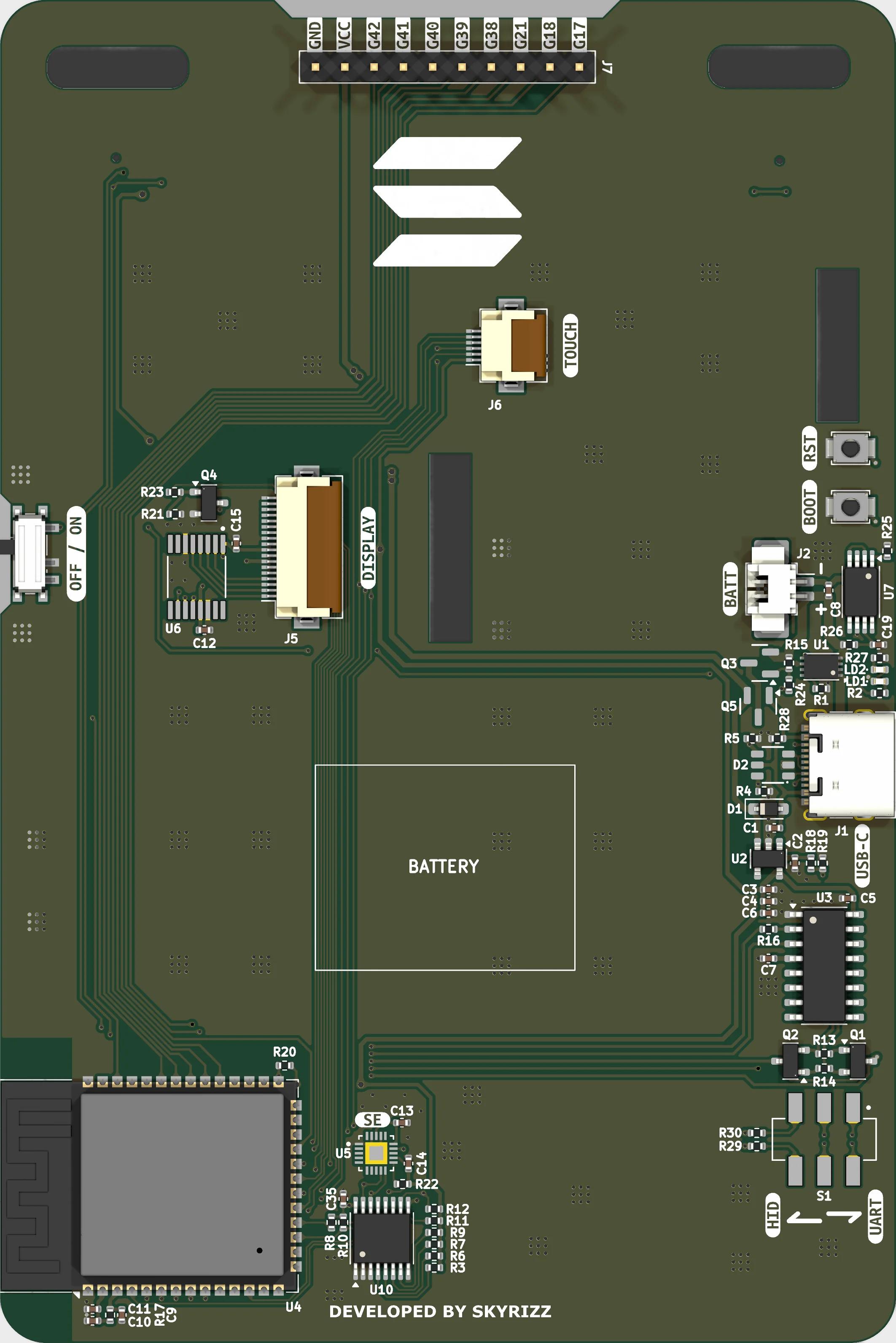
J7
← → to move between modules
09 / 09 · Expansion
J7 header
Eight free GPIO plus VSYS and ground on a 2.54 mm strip along the top edge.
- Connector
- 1×10, 2.54 mm
- GPIO
- 8 free
- Power
- VSYS + GND
- Edge
- Top
J7 runs along the top edge, exposing every GPIO the badge does not otherwise spend. Four of them double as the JTAG pins, so a debugger can go straight onto the header.
Pin 9 is VSYS rather than a regulated rail — whatever the power path is currently delivering, USB 5 V or battery voltage, after the ON/OFF switch. Regulate it yourself if your add-on needs something specific.
GPIO47 and GPIO48 used to be on this header. They now drive the microphones, so v1 carries 8 GPIO instead of 10.
Pins
| Pin | Net | Role | Function |
|---|---|---|---|
| 1 · GPIO17 | IO17 | J7 | Free GPIO (ADC2_CH6). |
| 2 · GPIO18 | IO18 | J7 | Free GPIO (ADC2_CH7). |
| 3 · GPIO21 | IO21 | J7 | Free GPIO. |
| 4 · GPIO38 | IO38 | J7 | Free GPIO. |
| 5 · GPIO39 | IO39 | J7 | Free GPIO (JTAG MTCK). |
| 6 · GPIO40 | IO40 | J7 | Free GPIO (JTAG MTDO). |
| 7 · GPIO41 | IO41 | J7 | Free GPIO (JTAG MTDI). |
| 8 · GPIO42 | IO42 | J7 | Free GPIO (JTAG MTMS). |
| 9 · — | VSYS | POWER | System rail before the 3V3 LDO, after the ON/OFF switch. |
| 10 · — | GND | POWER | Ground. |
Parts
- J7 Conn_01x10, 2.54 mm Expansion header