← → to move between modules
08 / 09 · Power
Battery and power path
Li-Po charging, protection, an ORing power path into a 3V3 LDO, and an ADC tap.
- Charger
- MCP73831 (U1)
- Protection
- DW03D (U7)
- Regulator
- ME6211C33 → 3V3
- Monitor
- GPIO1 · ADC1_CH0
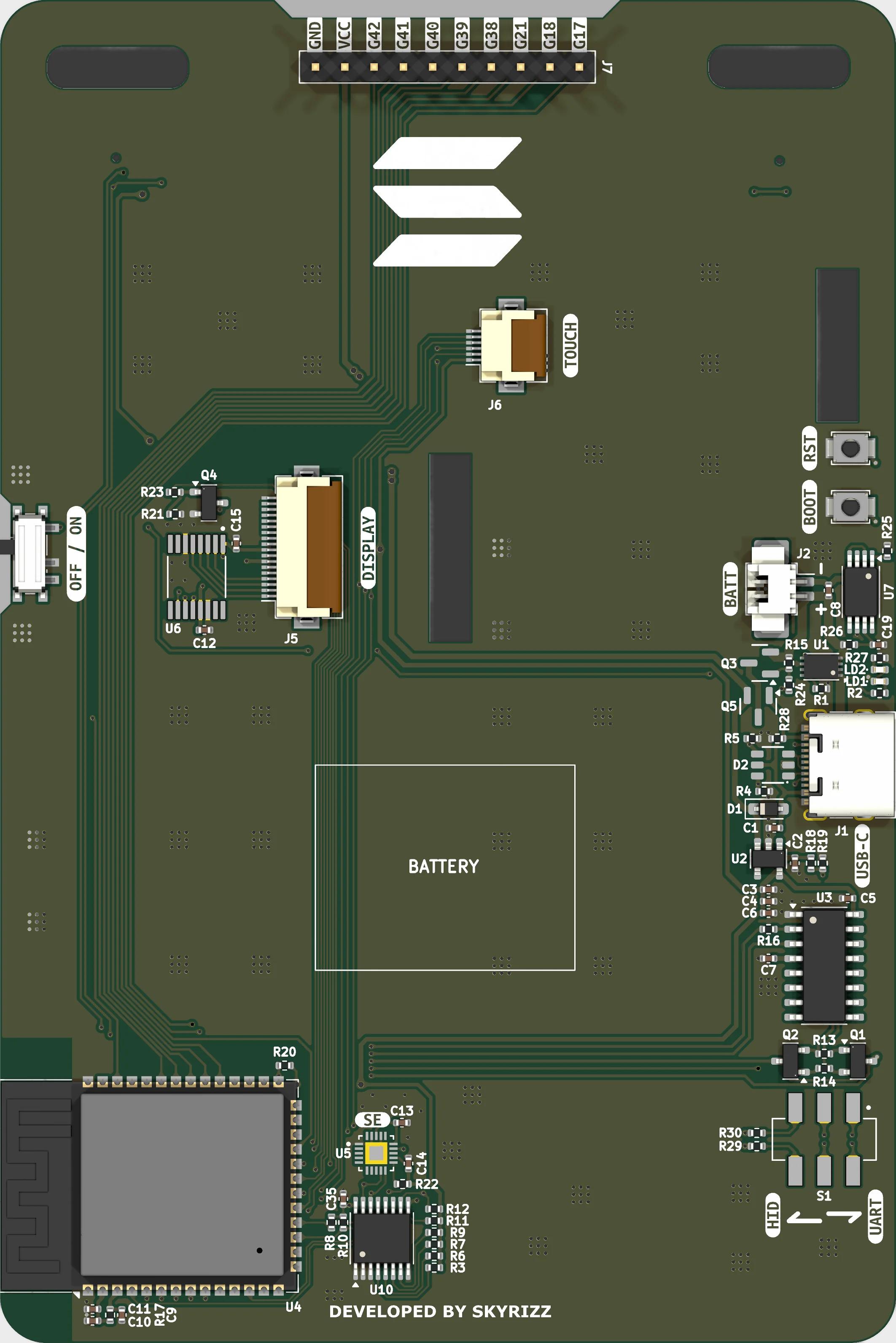
A Li-Po cell arrives on J2 through DW03D protection at U7, and U1 — an MCP73831 single-cell charger — tops it up whenever VBUS is present. LD1 and LD2 show charge state off the STAT net.
VSYS is where the two supplies meet. USB 5 V reaches it through Schottky D1 and Q5; the battery reaches it through Q3, an AO3401A P-channel FET gated by the ON/OFF slide switch. Whichever is higher wins, so the badge runs from USB when plugged in and hands over to the cell when unplugged without a reset. U2, an ME6211C33 LDO, drops VSYS to the 3V3 that feeds the module, the LCD, the microphones and the I²C devices.
Firmware can watch the rail: R18 and R19 form a 2K2/2K2 divider from VSYS into GPIO1 on ADC1_CH0. Double the reading to get VSYS. The same rail is exposed on J7 pin 9 if you want to power something from the badge.
Pins
| Pin | Net | Role | Function |
|---|---|---|---|
| GPIO1 | ADCBAT | ADC1_CH0 | VSYS through the R18/R19 divider (÷2). Multiply the reading by 2. |
Parts
- J2 MX1.25 2P Li-Po cell connector
- U7 DW03D Battery protection — over-charge, over-discharge, over-current
- U1 MCP73831-2 Single-cell Li-Po charger, status on the STAT net
- D1 BAT60A Schottky from VBUS into the power path
- Q3 / Q5 AO3401A P-channel FETs — battery path (switched) and USB path
- U2 ME6211C33M5 LDO — VSYS to 3V3
- ON/OFF_SW1 SS-203-AGS7P-200 Power slide switch on the left edge
- LD1 / LD2 LED red / blue Charge status indicators
Firmware
constexpr int PIN_BATTERY = 1; // VSYS / 2 on ADC1_CH0Notes
- Rails: VBUS (5 V from USB-C) · BAT (cell, after protection) · VSYS (VBUS ∥ BAT) · 3V3 (LDO output).