← → to move between modules
02 / 09 · Display
2.8" SPI LCD
ILI9341 240×320 panel on an 18-pin FPC, with a transistor-switched backlight.
- Panel
- ILI9341 240×320
- Bus
- SPI, 6 GPIO
- Connector
- J5 · 18-pin FPC
- Driver
- LovyanGFX
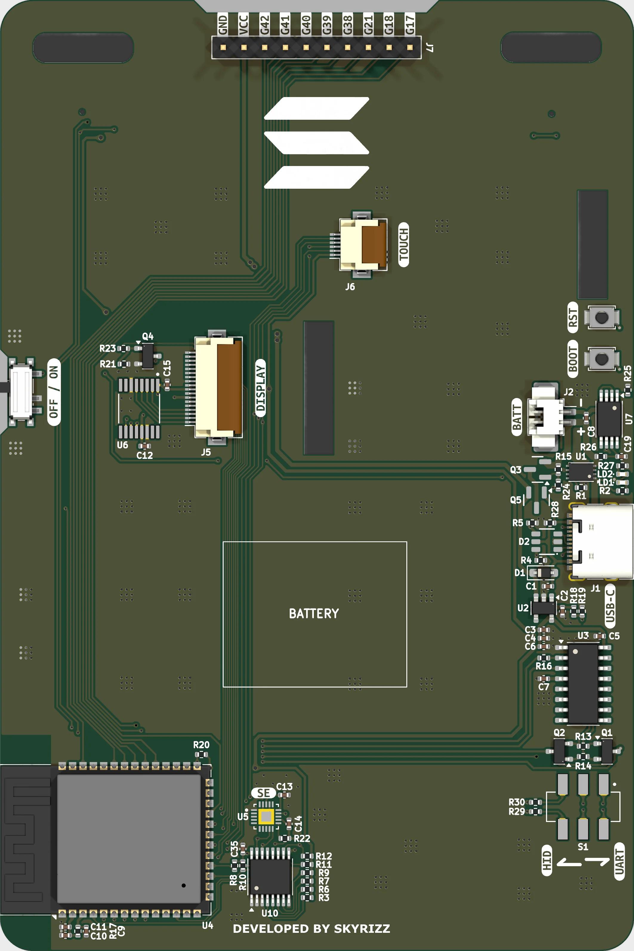
The panel plugs into J5, an 18-way FPC connector on the back face. Six GPIO carry a standard 4-wire SPI link — clock, MOSI, MISO, chip-select — plus a data/command select and a reset.
The backlight is not driven directly. GPIO7 goes through R23 into the base of Q4, an SS8050 NPN that sinks the four backlight LED cathodes on J5 pins 5–8. R21 pulls the base down so the backlight stays off until firmware asserts it. Because it is a transistor rather than a constant-current driver, PWM on GPIO7 is what gives you brightness control.
J5 pins 1–4 are the resistive touch lines. They are unused on this build — the panel is driven write-only in practice, so even MISO is optional.
Pins
| Pin | Net | Role | Function |
|---|---|---|---|
| GPIO7 | LCDBL | BACKLIGHT | Backlight enable / PWM. Drives Q4 through 10K R23, 470K pulldown R21. HIGH = on. |
| GPIO11 | LCDSCK | SPI CLK | SPI clock → J5 pin 16. |
| GPIO12 | LCDCS | SPI CS | Chip-select, active LOW → J5 pin 14. |
| GPIO13 | LCDDC | D/C | Data / command select → J5 pin 15. |
| GPIO14 | LCDRST | RST | Panel reset, active LOW → J5 pin 17. |
| GPIO15 | LCDMOSI | SPI MOSI | Data out, ESP32-S3 → LCD, J5 pin 13. |
| GPIO16 | LCDMISO | SPI MISO | Data in from LCD, J5 pin 12. Not required write-only. |
Parts
- J5 18-pin FPC, 0.5 mm Panel connector — SPI, backlight cathodes, 3V3, GND
- Q4 SS8050 NPN low-side switch for the backlight LEDs
- R23 / R21 10K / 470K Base resistor and pulldown for Q4
Firmware
constexpr int PIN_LCD_SCK  = 11;
constexpr int PIN_LCD_CS   = 12;
constexpr int PIN_LCD_DC   = 13;
constexpr int PIN_LCD_RST  = 14;
constexpr int PIN_LCD_MOSI = 15;
constexpr int PIN_LCD_MISO = 16;
constexpr int PIN_LCD_BL   = 7;

constexpr uint8_t LCD_ROTATION   = 1;
constexpr uint8_t LCD_BRIGHTNESS = 190;
Notes
- The touch panel is not documented or populated on this revision — J5 pins 1–4 (Y−/X−/Y+/X+) go nowhere useful.